As electronic devices continue to become more sophisticated, the demand for advanced circuit board manufacturing is rapidly increasing. In response to this demand, manufacturers are turning to High Density Interconnect (HDI) PCBs, a cutting-edge technology that allows for higher circuit density, smaller size, and lighter weight.
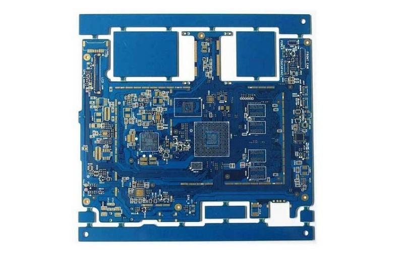
HDI PCBs are multilayered boards made of FR4 material with a thickness range of 0.2–10mm. They are characterized by their advanced surface treatment options, including Immersion Gold, ENIG, Immersion silver/Sn, HASL, and LF-HASL. HDI PCBs also feature stack up N+N technology, allowing for a higher number of layers and more complex circuits.
One of the most significant benefits of HDI PCBs is their ability to incorporate Blind and Buried vias and laser vias, which allows for a higher density of connections and more intricate circuitry. Additionally, HDI PCBs boast a minimum track/width of 3/3mil, allowing for greater precision and accuracy in the manufacturing process.
Manufacturers can choose from a variety of payment options, including L/C, T/T, and Western Union. HDI PCBs are also certified for use in a wide range of industries, including UL Consumer (Wear, Electronic Digital, Household Appliances, Connectors), Industrial Control, Automobile TS16949, Medical, Server, Cloud Computing & Base Station, Aviation, Military, and Communication.
In conclusion, HDI PCBs are a game-changer in the world of advanced circuit board manufacturing. With their advanced technology and cutting-edge features, they are well-suited to meet the demands of today’s fast-paced electronics industry.