In the ever-evolving world of electronics, the demand for smaller, faster, and more efficient devices has never been higher. High-Density Interconnect (HDI) Printed Circuit Boards (PCBs) have emerged as a game-changer in meeting these demands. HDI PCBs represent a technological leap that enables the development of sleeker, more powerful, and feature-rich electronic gadgets. This article explores the world of HDI PCBs, delving into their significance, manufacturing process, applications, and the impact they have on the electronics industry.
HDI PCBs: A Brief Overview
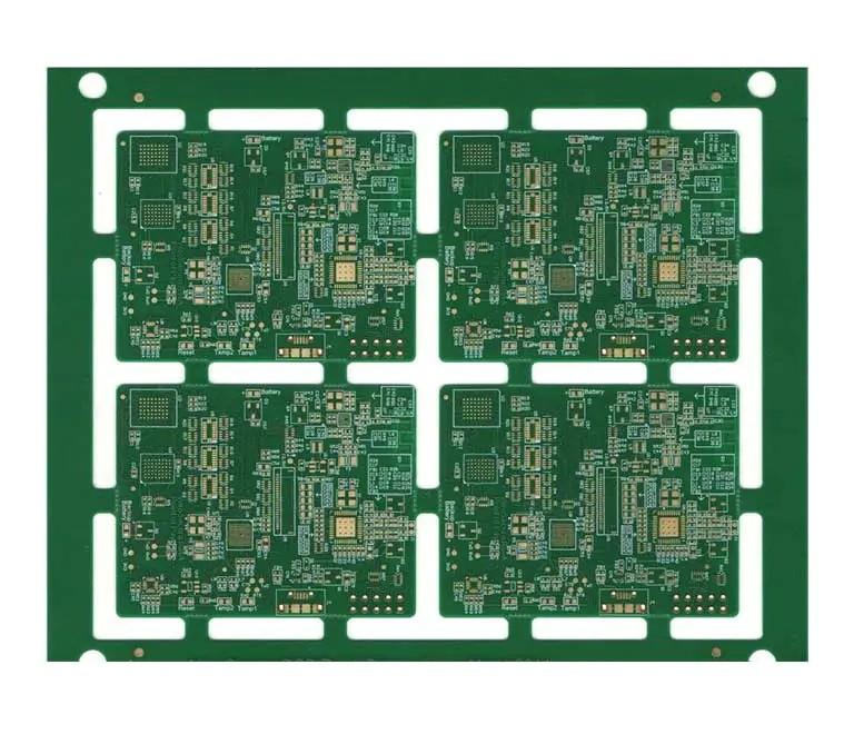
HDI PCBs are a specialized type of printed circuit board designed to optimize space usage and increase functionality. Unlike conventional PCBs, HDI PCBs offer a higher circuit density with multiple layers of closely packed components and traces. These boards are constructed using advanced manufacturing techniques, allowing for the creation of compact designs without compromising on performance.
The Manufacturing Process:
Creating HDI PCBs is a complex process that involves several stages. Here’s a simplified overview of the manufacturing process:
- Layer Stackup: HDI PCBs consist of multiple layers, including inner layers, outer layers, and vias (connections between layers). The stackup is carefully designed to accommodate the required circuitry and components.
- Laser Drilling: Laser drilling is a key step in HDI PCB manufacturing. It involves using laser technology to create small-diameter holes (microvias) that connect different layers of the board. This process allows for high-density component placement.
- Copper Plating: After drilling, the microvias are plated with copper to establish electrical connections between layers. This process ensures reliable signal transmission and power distribution.
- Surface Finishing: HDI PCBs are typically finished with various surface treatments, such as gold plating or solder mask, to protect the copper traces and improve solderability.
- Component Placement: SMT (Surface Mount Technology) is used to mount electronic components onto the PCB. Advanced pick-and-place machines precisely position tiny components, ensuring optimal space utilization.
Applications of HDI PCBs:
HDI PCBs have found their way into a wide range of applications across industries. Some notable applications include:
- Consumer Electronics: HDI PCBs are a cornerstone of smartphones, tablets, laptops, and wearable devices, enabling the compact design of high-performance gadgets.
- Medical Devices: Medical equipment, such as pacemakers, MRI machines, and diagnostic devices, rely on HDI PCBs for their compactness and reliability.
- Aerospace and Defense: HDI PCBs are crucial in aerospace applications, where size and weight constraints are significant factors.
- Automotive Electronics: The automotive industry uses HDI PCBs in advanced driver-assistance systems, infotainment systems, and engine control units.
- Industrial Automation: High-density PCBs are integral to the automation and control systems that drive modern factories and production lines.
Impact on the Electronics Industry:
HDI PCB technology has had a profound impact on the electronics industry in several ways:
- Miniaturization: HDI PCBs have enabled the development of smaller and sleeker devices, leading to innovations like foldable smartphones and ultra-thin laptops.
- Enhanced Performance: The high circuit density and optimized design of HDI PCBs result in improved signal integrity, reduced electromagnetic interference, and overall better performance.
- Cost-Efficiency: Despite their complexity, advancements in HDI PCB manufacturing have made these boards more cost-effective over time, making them accessible to a wider range of applications.
- Increased Functionality: HDI PCBs have opened the door to increased functionality in electronics, allowing for more features and capabilities in the same form factor.
Conclusion:
High-Density Interconnect (HDI) Printed Circuit Boards are a remarkable technological advancement that has revolutionized the electronics industry. Their ability to pack more functionality into smaller spaces has driven innovation across various sectors, from consumer electronics to aerospace and healthcare. As we continue to demand smaller, faster, and more efficient devices, HDI PCBs will remain at the forefront of this transformation, propelling us into a future filled with increasingly compact and powerful electronics