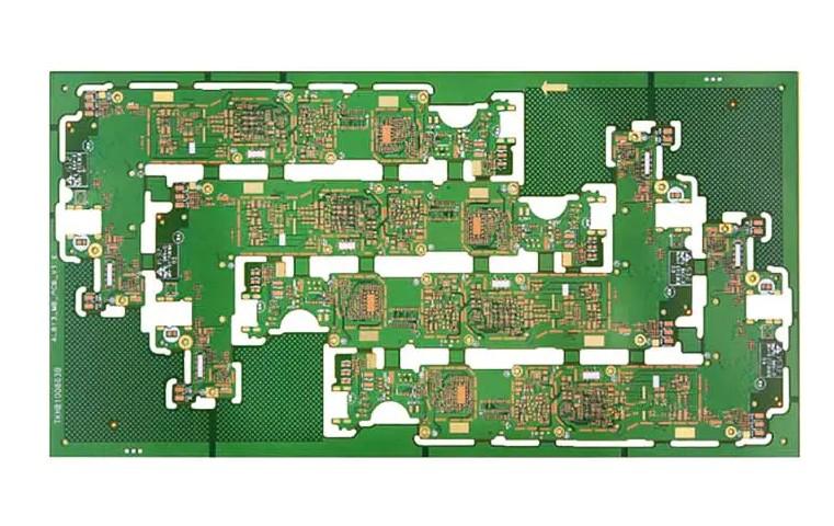
In today’s fast-paced technological landscape, printed circuit boards (PCBs) have become the backbone of nearly all electronic devices. The demand for smaller, more efficient, and high-performance PCBs is on the rise. To meet this demand, manufacturers are constantly pushing the boundaries of technology. One remarkable achievement in this regard is the fabrication of high-precision, any-layer HDI (High-Density Interconnect) multilayer PCBs. In this article, we’ll delve into the specifics of a cutting-edge 10-layer ELIC (Every Layer Interconnection) PCB, highlighting its key attributes such as materials, board thickness, surface treatment, and advanced manufacturing techniques.
Material Matters: FR4
The foundation of any PCB is its material, and in the case of our 10-layer ELIC PCB, FR4 (Flame Retardant 4) is the chosen substrate. FR4 is a widely-used material known for its excellent thermal stability, electrical insulation properties, and cost-effectiveness. It is a glass-reinforced epoxy laminate, providing the necessary mechanical strength and rigidity for complex multilayer boards like this one. FR4’s thermal properties ensure that the PCB can withstand the heat generated by various electronic components without compromising performance or reliability.
Precision in Thickness: 1.6mm
The thickness of a PCB plays a critical role in its overall performance. For this 10-layer ELIC PCB, a thickness of 1.6mm has been meticulously selected. This thickness strikes a balance between structural stability and the need to maintain a compact form factor. It allows for the board to fit into tight spaces within electronic devices while ensuring that it remains durable and reliable over time.
The Shimmer of Immersion Gold
Surface treatment is a vital aspect of PCB fabrication, and in this case, the PCB is treated with Immersion Gold. Immersion Gold, also known as ENIG (Electroless Nickel Immersion Gold), offers several advantages. It provides a flat and smooth surface finish, enhancing solderability. Additionally, Immersion Gold offers excellent corrosion resistance, ensuring that the PCB remains reliable even in challenging environmental conditions. This surface treatment is essential for high-precision applications where the integrity of electrical connections is paramount.
Technology at Its Peak: Advanced Stackup and More
To achieve the desired level of performance and miniaturization, advanced PCB fabrication technologies are employed in the making of this 10-layer ELIC PCB. The stackup used is N+N, signifying multiple layers that are closely connected. This allows for high-density interconnects between layers, reducing signal interference and maximizing signal integrity.
The minimum track width and spacing are an impressive 3/3mil (thousandths of an inch), showcasing the precision attainable with modern PCB manufacturing techniques. Such narrow tracks and spacing enable the PCB to accommodate densely packed components while maintaining the required electrical isolation.
Moreover, this PCB incorporates blind and buried vias. Blind vias connect an outer layer to one or more inner layers, while buried vias connect inner layers without extending to the outer layers. These vias allow for efficient routing of traces through multiple layers, reducing signal distortion and enhancing the overall performance of the PCB.
One of the standout features of this 10-layer ELIC PCB is the use of laser vias. Laser drilling is a high-precision technique that creates extremely small and precise holes for vias. This technology is crucial for achieving the high-density interconnect required for modern electronics. Laser vias contribute to the reduction of signal reflections and ensure that the PCB meets the stringent performance requirements of cutting-edge devices.
Conclusion
The 10-layer ELIC PCB, fabricated with precision and attention to detail, exemplifies the advancements in PCB technology. With its FR4 material, optimal thickness, Immersion Gold surface treatment, advanced stackup, and the inclusion of blind, buried, and laser vias, it is a testament to the relentless pursuit of excellence in the electronics industry. This PCB paves the way for smaller, more efficient, and high-performance electronic devices, proving that the future of technology lies in the hands of innovators who continue to push the boundaries of what is possible in PCB fabrication